A high-tech enterprise specializing in R&D and manufacturing of high-efficiency solar cells

Core values: Integrity cooperation for win-win development!
Business philosophy: All for the customer, all from innovation!
Corporate vision: To be the industry leader with the most investment value in the photovoltaic industry!
Enterprise spirit: Lean manufacturing, keep ingenious!
Enterprise talent view: Integrity and bright, passion and wisdom!


There is hope in light, technology is cohesive, we only do battery chips!
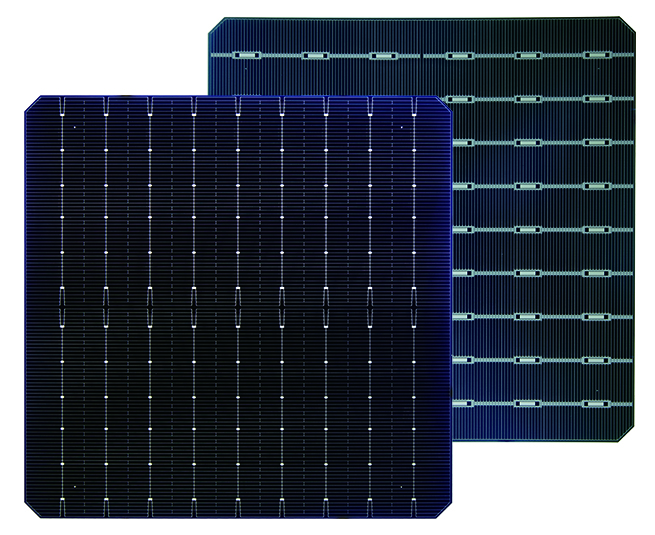
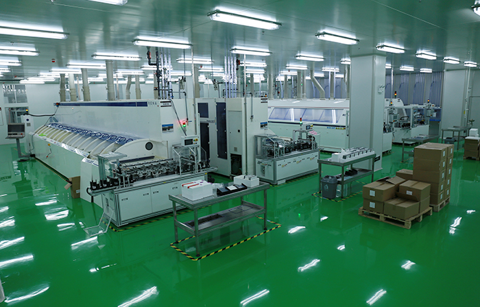
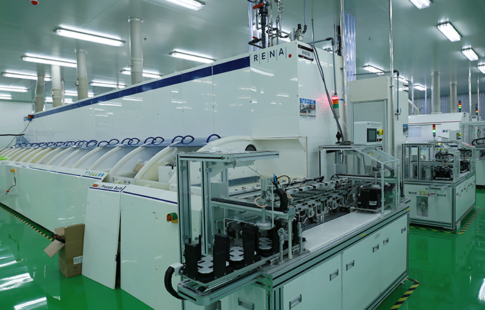
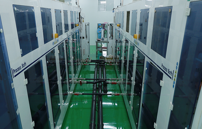
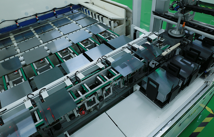
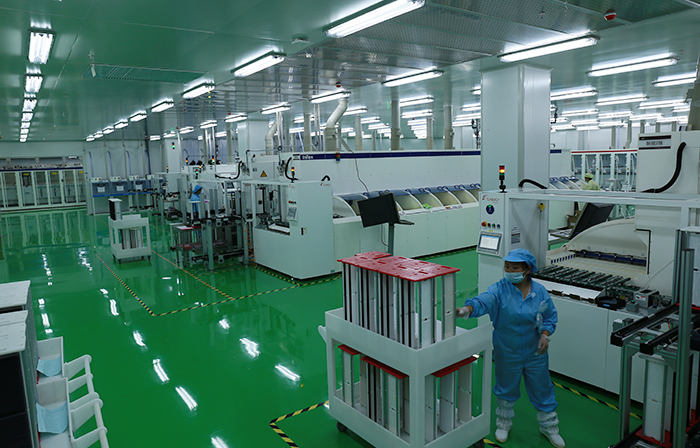
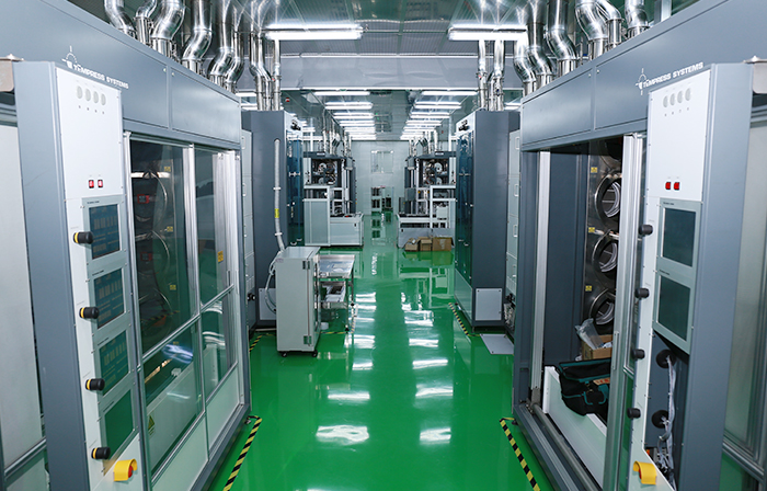
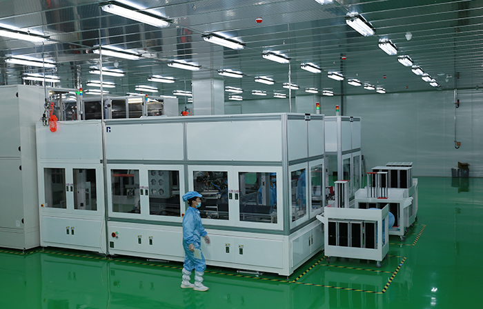
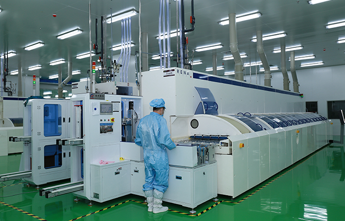
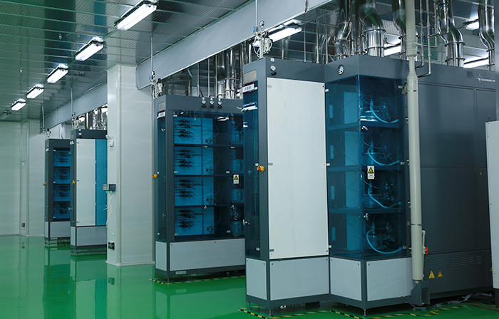
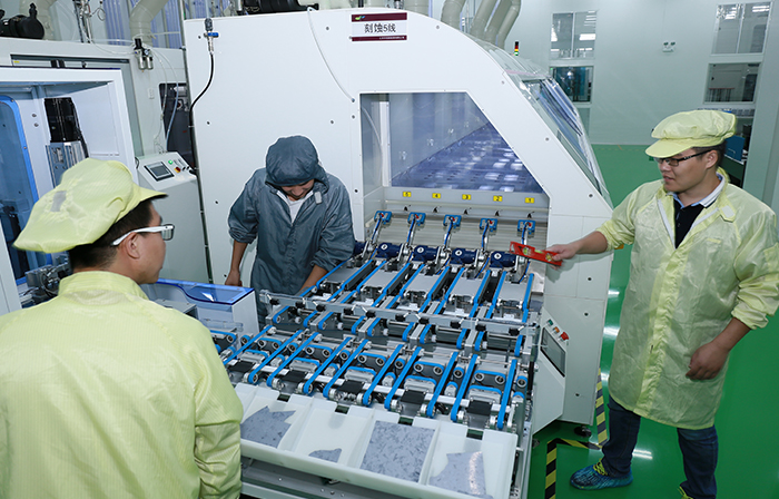
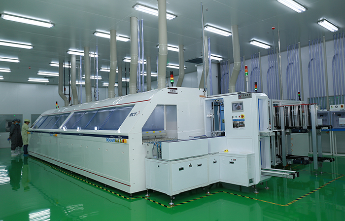
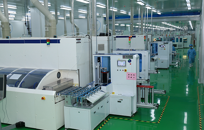
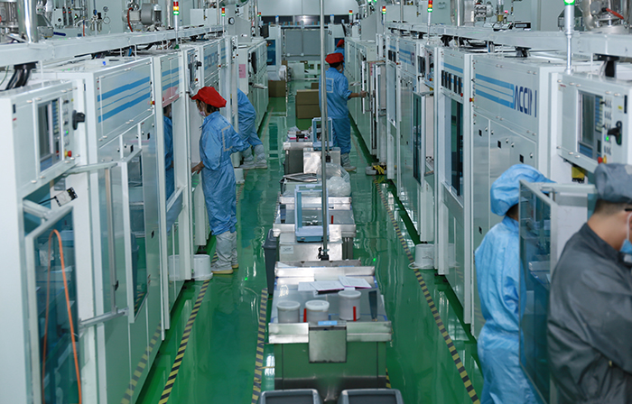
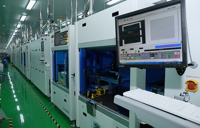
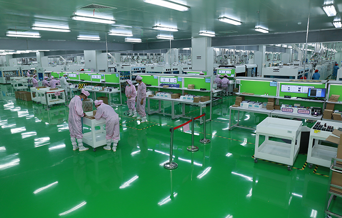
Process flow
The purpose of texturing is to form microstructures on the surface of silicon wafer (suede) and reduce the surface recombination of silicon wafer.
The purpose of diffusion is to form the PN junction on the surface of silicon wafer, which is the heart of the solar cells.
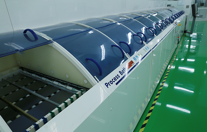
The purpose of etching is to remove the PN junction on the back and around the silicon wafer, and achieve the anti-PID function of the module through surface oxidation.
The purpose of PECVD is to form an anti-reflection film on the front of the silicon wafer, reduce the reflection of light, increase the absorption of light, and passivate the surface of the silicon wafer.
The purpose of screen printing is to form the electrodes of the cells, and the sintering process makes an ohmic contact between the metal electrode and the silicon.
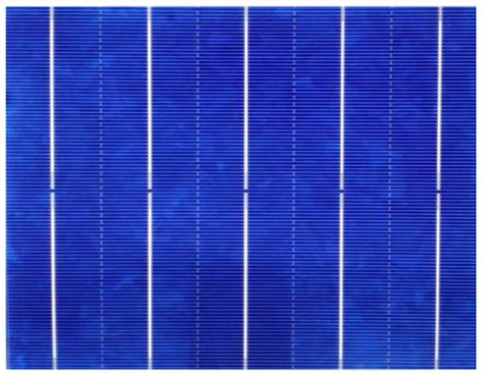
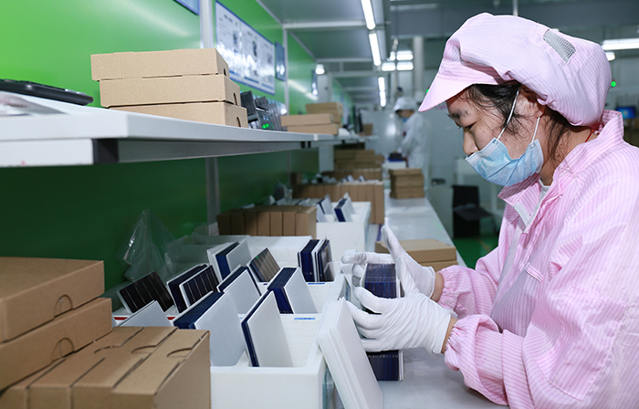
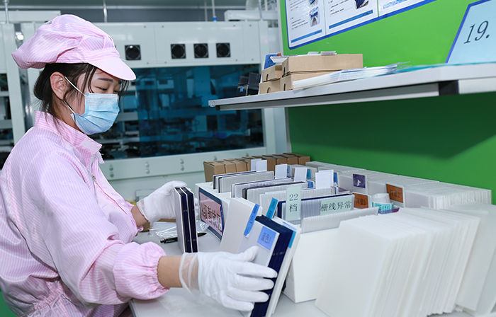
The cells with similar efficiency and color are sorted out and packaged together.
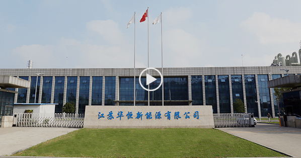
Recently, Jiangsu Huaheng New Energy Co., Ltd. successfully passed the national h…
According to the latest "China Solar Cell Export Data Report" released …
When the pace of construction of the domestic PV market slowed down, we were deli…
1. Keep ventilation Regardless of the components or the inverter, the distributi…
 Design Production:
all rights reserved :Jiangsu huaheng new energy co., LTD
design production:winsharing

 0516-68000566